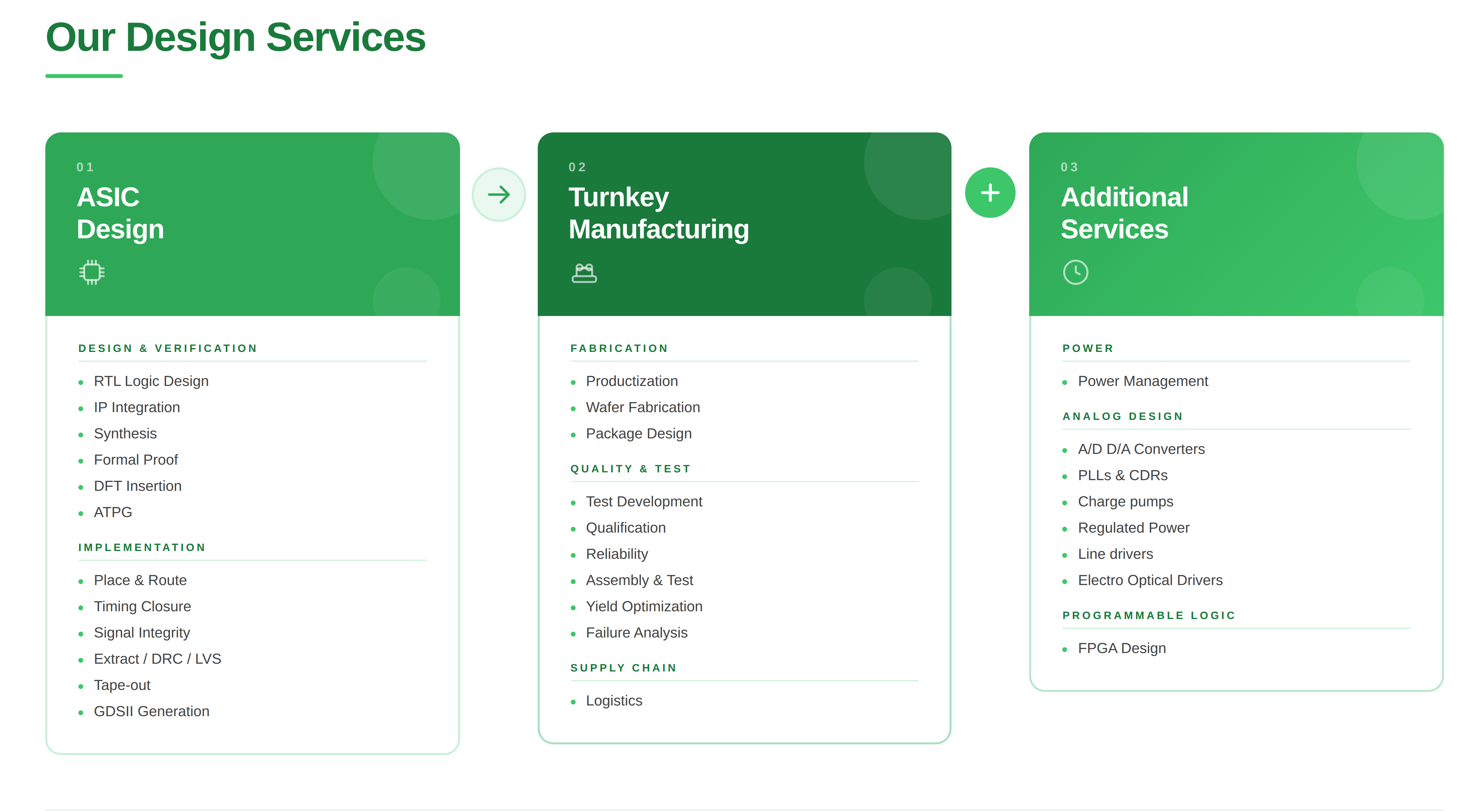
Our Design Team:
AAS maintains a strong in-house team with a wide variety of specialized skills in ASIC/SoC, analog and FPGA design; product engineering and production handling. Our team will help you not only to design the chip, but to find the best vendors for your project and to arrange a smooth tape-out and corner lot characterization. We'll develop for you the most attractive packaging solution and most efficient test program. Our team provides you with timely deliveries of superior quality products.
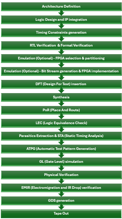
Design Flow:
AAS design methodologies expertise in ASIC and FPGA solutions enable us to achieve optimized designs in minimum iterations while meeting aggressive timing requirements and strict power budgets. The design methodology includes the following major steps:
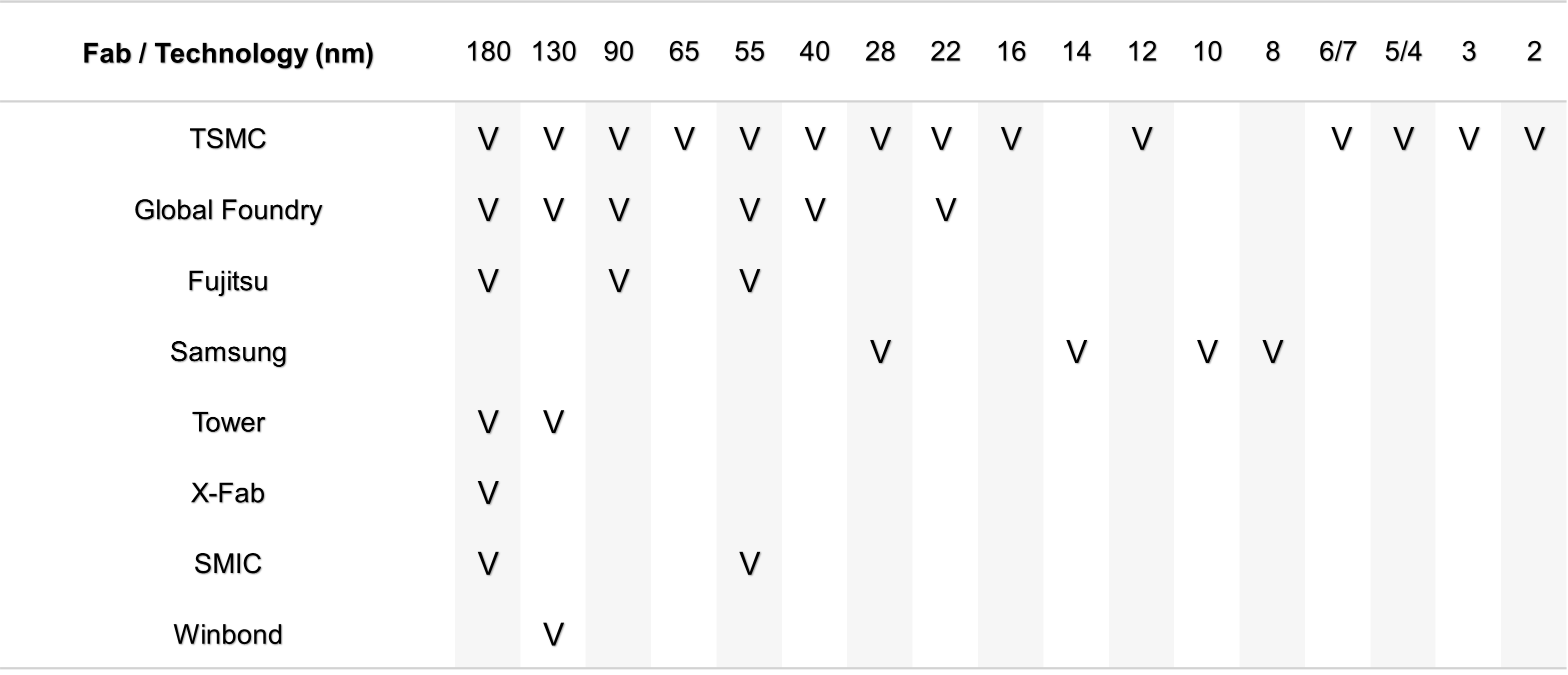
Fab / Technology Experience (Full Projects)
Design Platform:
Our design platform is based on Synopsys tools for RTL to GDSII flow and full custom analog design.
Our design team is well experienced with other advanced CAD tools, e.g. Cadence.
Our Design Partners:
Utilizing our in-depth industry knowledge and strong links with world-class semiconductor vendors, we grant our customers access to the most advanced design and manufacturing technologies, while providing more flexibility during the critical decision making process.
Quality Solutions & Support:
AAS offers a full range of quality solutions for the entire product life span. Yield optimization services include yield analysis, corner lot characterization, and process re-targeting. Complete support for new products is provided, including new product qualification, failure analysis, DPPM optimization and supplier change notification programs.
ISO 9001:2015 Certified.